Featured Post

80186 Microprocessors: Introduction and Architecture

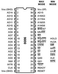
Hello friends, today we are going to discuss the 80186 microprocessor with integrated peripherals. The Intel 80186 is an improved version of the 8086 microprocessor. 80186 is a 16-bit microprocessor with a 16-bit data bus and a 20-bit address bus. It has a programmable peripheral device integrated into the same package. The instruction set of the 80186 is a superset of the instruction set of the 8086. The term super-set means that all of the 8086 instructions will execute properly on an 80186, but the 80186 has a few additional instructions. The following figure shows the block diagram and pin diagram of 80186. The CPU is divided into seven independent functional parts. 80186 internal block diagram  80186 68-pins pin diagram  Functional parts of 80186 Microprocessor The Bus Interface Unit (BIU) Execution Unit (EU) Clock Generator Programmable interrupt controller Programmable Chip Select Unit (CSU) Programmable DMA Unit Programmable counter/timers The Bus Interface Unit

Pin Diagram Of 8086 Microprocessor

Hello friends, today we are going to discuss pin diagram of microprocessor. We already seen the internal architecture of 8086 microprocessor, if you missed the post to see here is a link please check. The 8086 Microprocessor - Internal Architecture.

Pin Diagram of 8086

The 8086 is a 16-bit microprocessor intended to be used as the CPU in a microcomputer. Following figure shows the logical pin diagram of 8086 microprocessor. All the signals can be classified into six groups:


  • Power supply and frequency signals
  • Clock signal
  • Address bus
  • Data bus
  • Mode selection.
  • Control and status signals
  • Externally initiated signals, including interrupts
Pin diagram of 8086 microprocessor
Pin Diagram Of 8086


Power supply and frequency signals

Vcc is on pin 40 supplies +5V power supply.
Pin 1 and 20 for ground reference.

Clock signal

Pin 19 for clock input (CLK): an 8086 requires a clock signal from some external, crystal-controlled clock generator to synchronize internal operations in the processor with maximum frequencies ranging from 5 MHZ to 10 MHZ.

Multiplexed address/data Bus

AD0 through AD15 are used at the start of machine cycle to send out addresses and later in the machine cycle they are used to send or receive data. (This is also known as multiplexing the bus.) However, the-low order address bus can be separated from these signals by using a latch.

Multiplexed address bus

The 8086 has 4 signal lines A16/S3 through A19/S6. The double mnemonic on these pins indicates that address bits A16 through A19 are sent out on these lines during the first part of a machine cycle and the status information, which identifies the type of operation to be done in that cycle, is sent out on these lines S3 through S6 during a later part of the cycle.

Mode selection

The operating mode of the 8086 is determined by the logic level applied to the MN/MX input on pin 33. If pin 33 is asserted high, then the 8086 will function in minimum mode, and pins 24 through 31 will have the functions shown in parentheses next to the pins i.e. INTA, ALE, DEN, R, M/IO, WR, HLDA, and HOLD. If the 8086 is in minimum mode in systems, it works as a single microprocessor on the system buses.
If the MN/MX pin is asserted low, then the 8086 is in maximum mode. In this mode pins 24 through 31 will have the functions described by the mnemonics next to the pins i.e. QS1, QS0, S0, S1, S2LOCK, GT1, RQ, GT0 . If the 8086 is in maximum mode in systems, it has two or more microprocessors sharing the same buses and this mode is called multiprocessor mode.

Control and status signal

This group of signals is to identify the nature of the operations. These signals are as follows.

  • ALE- Address Latch Enable (pin 25): this is a positive going pulse generated every time the 8086 begins an operation (machine cycle).This output signal indicates the availability of the valid address is on the address/data lines.
  • RD (pin 32) Read: This is read control signal (active low). This signal indicates that the selected I/O or memory device is to be read and data are available on the data bus.
  • WR (pin 29) Write: This is a write control signal (active low). This signal indicates that the data on the data bus are to be written into a selected memory or I/O location.
  • MIO (Pin 28): when it is high, reading from and writing to a memory location, and if it is low, reading from and writing to a port.
  • \S0, S1, S2(pins 26, 27 and 28): these control bus signals are sent out encoded form of data and an external bus controller device decodes these signals to produce the control bus signals required for a system which has two or more microprocessors sharing the same buses.
  • DEN(pin 26) Data Enable signal: it is used to enable bidirectional buffers on the data bus, when DEN is low. i.e. it send data out on the data bus and read the data in on the data bus.
  • DT/R (pin 27) Data transmit/receive signal: when DT/R is high, the 8086 is used to decide the direction in which the buffers are enabled through the DEN the 8086 transmit the data to ROM, RAM, or ports. when DT/R is low, the buffers will allow data to come in from ROM, RAM, and ports.
  • BHE/S7 (pin 34) Bus high enable: The bus high enable is used to indicate the transfer of data over the higher order data bus If it goes low, the address that it will be writing to on AD0 - A19.


Interrupts and Externally initiated signals

  • NMI (Nonmaskable interrupt pin 17) and INTR (interrupt pin 18) input :A signal can be applied to one of these inputs to cause the 8086 to interrupt the program it is executing and go execute a specified procedure.
  • HOLD input (pin 31): when the HOLD line is high , this signal indicates that a peripheral such as a DMA (DMA Direct memory Access) controller is requesting the use of the address and data buses.
  • HLDA (pin 30) Hold Acknowledge: This signal acknowledges the HOLD request.
  • READY input (pin 22): This signal is used to delay the microprocessor Read or Write cycles until a slow responding peripheral is ready to send or accept data. When this signal goes low, the microprocessor waits for an integral number of clock cycles until it goes high.
  • RESET (pin 21): This signal indicates that the MPU (microprocessor) is being reset. The signal can be used to reset other devices.
Well, how you found this article, is this useful? I'm sure this will help you more. If you want more information please let me know through comments in the right below.Subscribed to the My Computer Tutors for updates. I will keep updating to you with latest tutorials.

Comments

  1. Sagar Rathod4/14/2012

    Gr8 Website..

    2morrow is my microprocessor's paper and i m studying from here...

    best notes ever:)

    ReplyDelete
  2. Easy to understand 8086 pins functions.

    ReplyDelete

Post a Comment

Your comment will inspire me, Please leave your comment