Hello friends, today we are going to discuss the 80186 microprocessor with integrated peripherals.
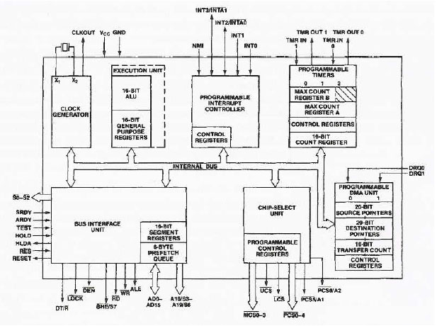
The Intel 80186 is an improved version of the 8086 microprocessor. 80186 is a 16-bit microprocessor with a 16-bit data bus and a 20-bit address bus. It has a programmable peripheral device integrated into the same package. The instruction set of the 80186 is a superset of the instruction set of the 8086. The term super-set means that all of the 8086 instructions will execute properly on an 80186, but the 80186 has a few additional instructions. The following figure shows the block diagram and pin diagram of 80186. The CPU is divided into seven independent functional parts.

80186 internal block diagram

80186 68-pins pin diagram
In addition to producing memory chip select signals, the 80186 can be programmed to produce up to seven peripheral chip select signals on its PCS0 -PCS4, PCS5/A1, and PCS6 /A2 pins. The programmable I/O area starts at a base I/O address programmed by the user, and all seven 128-byte blocks are contiguous.
How you found this article, is it useful? please feel free to write me a comment so I can improve for the betterment. If you would like more information please visit our other posts or let me know through comments in the right below.
Subscribed to the My Computer Tutors for updates. I will keep updating to you with latest tutorials.
The Intel 80186 is an improved version of the 8086 microprocessor. 80186 is a 16-bit microprocessor with a 16-bit data bus and a 20-bit address bus. It has a programmable peripheral device integrated into the same package. The instruction set of the 80186 is a superset of the instruction set of the 8086. The term super-set means that all of the 8086 instructions will execute properly on an 80186, but the 80186 has a few additional instructions. The following figure shows the block diagram and pin diagram of 80186. The CPU is divided into seven independent functional parts.
80186 internal block diagram
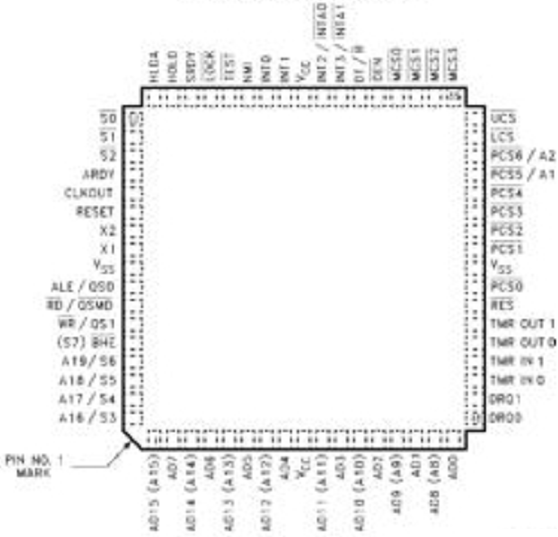
80186 68-pins pin diagram
Functional parts of 80186 Microprocessor
- The Bus Interface Unit (BIU)
- Execution Unit (EU)
- Clock Generator
- Programmable interrupt controller
- Programmable Chip Select Unit (CSU)
- Programmable DMA Unit
- Programmable counter/timers
The Bus Interface Unit (BIU)
The 80186 has the same bus interface unit (BIU) and execution unit (EU) as the 8086. We can see this under the heading The 8086 Microprocessor- Internal Architecture. The 80186 is 68 pins lead-less package, so it has enough pins to send out both the minimum mode type signals RD and WR and the S0 – S3 status signals which can be connected to external bus controller ICs for maximum mode systems. It does not have a pin labeled MN/MX for switching the minimum mode through the maximum mode.Clock Generator
The 80186 has a built-in clock generator so that we can add external crystal. This reduces the component count in a system. It has three-pin connections: X1, X2, and CLK OUT. The X1 and X2 pins are connected to a crystal that resonates twice the operating frequency of the microprocessor. The CLK OUT pin provides a system clock signal that is one-half the crystal frequency. In addition to external pins, the clock generator provides the internal timing for synchronizing the READY input pin.Programmable Interrupt Controller
The programmable interrupt controller has four interrupt inputs: INT0, INT1, INT2/INTA0, and INT3/INTA1 as well as one nonmaskable interrupt NMI input. These inputs operate with two modes: internal mode and external mode. In internal mode, if the four INT inputs are programmed, then a signal is applied to one of them to push the return address on the stack and vector directly to the start of the interrupt service procedure for that interrupt. In external mode, the INT2/INTA1 pins can be programmed to be used as interrupt inputs or they can be programmed to function as an interrupt acknowledge outputs. This mode is used to interface with external 8259As. When the 8259A is externally attached to 80186, the 80186 microprocessors work as the master, and the 8259A works as the slave.Programmable Chip Select Unit
This built-in address decoder unit can be programmed to produce an active low chip select signal when the memory or port address in a specified range is sent out. This built-in decoder is to select major blocks of memory. six memory address chip select signals are available: lower chip select lines LCS upper chip select lines UCS and middle chip select lines MCS 0-3 The boundary of the lower chip select signal begin at location 00000H and the boundary of the upper chip select signal is ends at location FFFFFH. The sizes of the memory areas are programmable by some bits put in a control word, and wait states (0-3 waits) can be automatically inserted with the selection of an area of memory.In addition to producing memory chip select signals, the 80186 can be programmed to produce up to seven peripheral chip select signals on its PCS0 -PCS4, PCS5/A1, and PCS6 /A2 pins. The programmable I/O area starts at a base I/O address programmed by the user, and all seven 128-byte blocks are contiguous.
Programmable DMA Unit
The DMA unit has two DMA request inputs, DRQ0 and DRQ1. These inputs allow external devices such as disk controllers, CRT controllers, etc. to request the use of one of the DMA channels. For each DMA channel, the 80186 has a full 20-bit register to hold the source address, a 20-bit register to hold the destination address, and a 16-bit counter to keep track of how many words or bytes have been transferred. DMA transfers can be from memory to memory, I/O to I/O, or between I/O and memory.Programmable counter/timers
The timer section contains three fully programmable 16-bit timers. Timers 0 and 1 generate waveforms for external use and are driven by either the master clock of 80186 or by an external clock. They are also used to count external events. The third timer, timer 2, is internally connected to the processor clock. The output of timer 2 generates an interrupt after a specified number of clocks and can provide a clock to the other timers.How you found this article, is it useful? please feel free to write me a comment so I can improve for the betterment. If you would like more information please visit our other posts or let me know through comments in the right below.
Subscribed to the My Computer Tutors for updates. I will keep updating to you with latest tutorials.
I got here much interesting stuff. The post is great! Thanks for sharing it! Microprocessor and Peripherals
ReplyDeleteNeed some more information like multitasking ability.... Pipelining?
ReplyDeletevery much interesting please keep it up ..
ReplyDeleteI admire this article for the well-researched content and excellent wording. I got so involved in this material that I couldn’t stop reading. I am impressed with your work and skill. Thank you so much. antminer s17
ReplyDeletemuch helpful content
ReplyDelete